Atlas, 
LHCb,
RD50. Some of the work I have
performed in the framework of these experiments can be found below.
 
 Radiation tolerance of silicon detectors
| 
The silicon detectors will provide the main tracking capability for the future experiments in high-energy physics. In most of these experiments they will have to withstand a harsh radiation environment. The survival of the detectors to the severe radiation fluences they will receive is a challenge for the detector technology. We are involved in the development of the sensors for several of the major experiments that will take place in CERN-LHC (ATLAS, LHCb) and FERMILAB (CDF). In this page I have collected several results concerning the study of silicon detectors mainly on the subject of their radiation hardness. 
 |   
 
 SCT ATLAS sensors page: a systematic study of the radiation 
behaviours of the sensors for the ATLAS tracker has been 
carried out for a few years. The Liverpool University was heavily involved in this program. 
A number of results obtained within this program is collected in the following section:
 
pre and post irradiation characterisation of SCT ATLAS sensors.
 
 Studies for CDF Tests for the commissioning of the Layer00
for the CDF experiment have been carried here. Results are reported in my 
CDF-L00 page.
 
 Studies for LHCb-VELO Tests for the commissioning of the Layer00
for the CDF experiment have been carried here. Results are reported in my 
LHCb VELO page. 
The study of irradiated devices is key part of the work. The  
irradiation 
plans for LHCb VELO can be found here. 
 
CERN RD50 
(Radiation hard semiconductor devices for very high luminosity colliders): I am the convener of the Full 
Detector Systems research line of the CERN-RD50 collaboration. To see the 
scope and the participant institutes to this collaboration 
click here. You can follow the link to find the list some of the 
contribution I gave to the  RD50 meetings and workshops.
 
 
 Oxygen enrichment technique
I've conceived the high temperature diffusion technique to introduce
high concentrations of oxygen into silicon wafers. This development was
done in the frame of RD48 collaboration. It can be used for other fast
diffusing element in silicon. You find  
here the description of this technique. 
 Also look in: http://rd48.web.cern.ch/RD48/, Technical Reports page, ROSE/TN/99-1.
 You can find further details in Chapter
5 and Appendix B of my PhD
thesis.
 |   
 
 Effect of oxygen enrichment on silicon detectors
The high temperature diffusion technique, as described above, is a cheap way to achieve a significant enhancement of the
oxygen content in Float Zone silicon wafers. How much does it affect the performances of the devices? At first, very simple devices (pad diodes) were produced with 
oxygen enriched material and compared to 'standard' FZ silicon. Nonetheless the 
results obtained with simple pad diodes are not fully representative of the 
performances of the finely segmented detectors used in the experiments. We 
pioneered the studies of segmented oxygen enriched detectors. Miniature and full 
size oxygen enriched and standard segmented detectors were produced. We 
characterised various type of segmented devices in term of the changes of their 
performances after irradiation. Many parameters have been monitored (I-V, C-V, 
interstrip capacitance and mainly CCE).  The following pages report some of 
those results: 
Oxygenated diode page.
 
Large area 
and miniature segmented detectors 
 
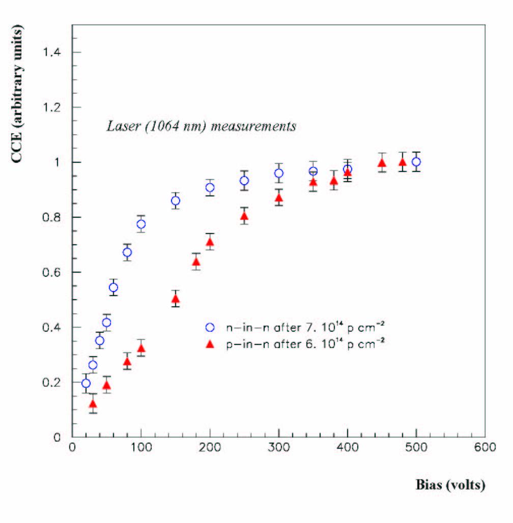
In the development of silicon microstrip detectors for high 
energy physics applications the Liverpool laboratory clearly established the 
advantage of reading out finely segmented devices from the n-type implants.
Silicon detectors made with n-type bulk silicon undergo space 
charge sign inversion after being irradiated with hadron to a dose of a few 1013 
cm-2  The standard diode structure for segmented detectors used 
in high energy physics is p-strips implanted into a lightly doped n-type 
substrate. With this geometry, after type-inversion, the high electric field is 
on the opposite side to the read-out strips, resulting in a reduced charge 
collection vs bias (CCE(V)) at low voltages. The CCE(V) can be improved by 
segmenting and reading out the n-side of the detector (n-in-n geometry). Very 
good performance after irradiation has been achieved with this geometry. 
An example of the advantages of this geometry is 
shown here. The n-side 
read-out concept is now widely accepted. The most exposed silicon detectors of 
the LHC experiments (ATLAS and CMS pixels and LHCb-VELO microstrips) all use 
n-side read-out. 
 
The 
limitation with the n-in-n devices is the higher processing cost, and, to a 
lesser extent, that the junction side (and the high electric field) is on the 
opposite side before irradiation. Both the migration of the junction after type 
inversion and the extra cost due to the double-sided processing can be avoided 
by using a p-type bulk substrate. Concerning the CCE(V) properties as a function 
of the cumulated fluence, an improvement similar to the n-in-n read-out was 
expected with p-type substrates. To investigate this issue we first produced 
ATLAS SCT geometry, p-type substrate detectos with p-stop interstrip isolation. 
The production was successful and proved the feasibility and the improvements of 
this solution. The irradiation fluence was up to LHC tracker levels (~ 4. 1014 
p cm-2). To further study the radiation hardness of these detectors 
to super-LHC levels we produced miniature n-in-p capacitively coupled, 
polysilicon biassed microstrip detectors (1x1 cm-2, 100 strips). 
These miniature devices allowed us to investigate the charge collection 
properties up to 7.5 1015 p cm-2. I report here the 
extremely positive results we have obtained.  
P-type detectors page. 
 
RECENT PUBLICATIONS AND TALKS
  Some of this material has been put together for conference presentations 
and/or articles. Here I list some recent presentations. 
  
 
  | 
   
  VERTEX 2008 
   | 
  
   …or the 17th International Workshop on Vertex 
  Detectors, 
	Utö Island, Sweden,
 
	July 28–August 1, 2008. You find here the talk. 
   | 
  
 
  | 
  Barcelona 2008 | 
  
  .....or the 3rd 
	Workshop on Advanced Silicon Radiation Detectors (3D and P-type 
	Technologies), Barcelona 14-16 April 2008. | 
	 
 
  | 
  INSTR08 | 
  
  ..... or the 10th 
	International Conference on Instrumentation for Colliding Beam Physics, 
	Budker Institute of Nuclear Physics, Siberian Branch of Russian Academy of 
	Science, Novosibirsk, Russia, February 28 - March 5, 2008. | 


  | 
  VLC2007 | 
  
  .....or the ATLAS 
	Tracker Upgrade Workshop, Valencia (SP), 12-14 December 2007. | 
	 
 
  | 
  IEEE 2007 | 
  
  ..... or the Nuclear 
	Science Symposium and Medical Imaging Conference, October 27 – November 3, 
	2007, Honolulu (Hawaii), USA. 
  ou can find here my article. | 


  | 
  VERTEX 2007 | 
  
  ...... or the 16th International Workshop on Vertex detectors, September 
	23-28, 2007, Lake Placid, NY, USA.
  You can find here my talk | 


  | 
  9th IWORID | 
  
  ....or the 9th International Workshop on Radiation Imaging Detectors, Erlangen, 
	Germany 22-26 July 2007.
   
  You can find here my talk. | 


  | 
    VCI 2007 
   | 
  
    …or the  11th Vienna Conference on 
  Instrumentation, Vienna, Austria, February 19-24 2007. 
	 
   | 


  | 


  AHLUTW


  '06 
   | 
  
   …or the 
  
  ATLAS High Luminosity  Upgrade Tracker Workshop, Liverpool: 6 - 8 
  December 2006.You find here my talk. 
   | 


  | 
    STD6 
   | 
   
  
   ... or 6th International 
  “Hiroshima” Symposium on the Development and Application of Semiconductor 
  Tracking Detectors, see
  
  http://scipp.ucsc.edu/STD6/. You can find here my
  talk.  
   | 


  | 
   
  TIME'05 
   | 
  
   …or the Workshop on Tracking In 
  high Multiplicity Environments, 
  October 3-7, 2005, Zurich, Switzerland. You find here the talk. 
   | 


  | 
    Genova 
  '05 
   | 
  
   ... the ATLAS tracker upgrade 
  workshop, in Genova (Italy) 18-20 July 2005, see
  
  http://agenda.cern.ch/fullAgenda.php?ida=a053875. You can find here my
  talk.  
   | 


  | 
   
  Kreuth 
  
  '05 
   | 
   
  
   …or the 
  10th European 
  Symposium on Semiconductor Detectors, 
   
  June 
  12 - 16, 2005, Kreuth ,
   
  Germany. You find here the
  talk. 
   | 


  | 
   
  RESMDD'04 
   | 
  
   …or the  5th International Conference on 
  Radiation Effects on Semiconductor Materials Detectors and Devices October 
  10-13, 2004, L.go E. Fermi 2, Florence, Italy.  You find here the talk. 
   | 
  
  | 
   
  VCI 2004 
   | 
  
   …or the  10th Vienna Conference on 
  Instrumentation, Vienna, Austria, February 16-21 2004. You find here the article. 
   | 
  
 
  | 
   
  ERICE 2003 
   | 
  
   …or the workshop on Innovative Detectors for 
  Supercolliders, Erice (TP), Italy, 29th Sep.-03 Oct. 2003.  You find here the talk 
  and the article. 
   | 
  
 
  | 
   
  ELBA 2003 
   | 
  
   …or the 9th Pisa Meeting on Advanced Detectors, La 
  Biodola, Isola d'Elba, 25-31 May 2003  November 3-8, 2002. You find here the poster 
  and the article. 
   | 
  
 
  | 
   
  VERTEX 2002 
   | 
  
   …or the 11th International Workshop on Vertex 
  Detectors, Ohana Keauhou Beach Resort, 78-6740 Alii Drive Kailua-Kona, 
  Hawaii  November 3-8, 2002. You find here the talk 
  and the article. 
   | 
  
 
  | 
   
  ELMAU 2002 
   | 
  
   … or the  9th European Symposium on Semiconductor 
  Detectors, New Developments on Radiation Detectors, Schloss Elmau, June 23 - 
  27, 2002. You find here the article. 
   | 
  
 
  | 
   
  ISM2E-YS  
   | 
  
   ... invited talk at the International 
  Symposium of Young Scholars on Mechanical and Material Engineering for Science 
  and Experiments, 11-16th of August 2001 Changsha, Hunan Province, China. Here 
  you can find the transparencies of my talk.  
   | 
  
 
  | 
   
  4th STD  
   | 
  
   ... or the 4th International Symposium on 
	Development and Application of Semiconductor Tracking Detectors (Hiroshima, 
	March 22-25 2000). Here you can 
  find the transparencies of my talk.  
   | 
  
 
  | 
   
  RD 99  
   | 
  
   ... or the 4th International Conference on 
  Large Scale Applications and Radiation Hardness of Semiconductor Detectors (Firenze, 
	Italy, 23-25 June 1999).
  Here you can find the article.  
   | 
  
 
  | 
   
  Radecs 99 
   | 
  
   ....or the 5th EUROPEAN CONFERENCE: 
  Radiation and its effects on components and systems (Abbaye de Fontevraud, 
  FRANCE, Maine et Loire, 13 - 17 septembre 1999).
  Here you can find the poster  
  and the article.  
   | 


| 
 
SEMINARS  
  
    | 
    University of Glasgow | 
    
    06/12/2007, Here is the
	talk. | 
   
  
    | 
     
    University of 
    
    Bonn  | 
    
     15/12/2005, Here is the
    talk.  | 
   
  
    | 
     IFIC-Valencia  | 
    
     21/05/2004, Here is the
    talk.  | 


If you want to take a look to my thesis 
(again on silicon detectors)
  
 PhD 
thesis (Université Joseph Fourier - Grenoble I, France):  
The effect of hadron irradiation on the 
electrical properties of particle detectors made from various silicon materials. 
 N.B. Text is in English.  
 
My   
Publication List.
 
 
For comments etc. please contact 
Gianluigi Casse 
 
 Contact Information  
 
 
Last modified:
07/08/2008 
 |  
    |  
    |