"Development of the front-end."
|
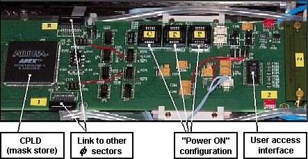
Every motherboard supervises 8 detector modules. This
includes: setting thresholds, generating, downloading,
reading back and verifying sequencer codes, issuing
calibration pulses, receiving and processing trigger
signals. One card is equipped with two complex
programmable logic devices (CPLD): the "ACEX" EP1K30
for the slow control and the "APEX" EP20K300E for the
online trigger data analysis. The JTAG protocol was
chosen to configure CPLDs and their EPROMs. This
electrical standard allows exchanging the default and
the pilot firmware during the trigger system operation.
The user access to the front-end is organized via the
standard serial line input-output interface (SLIO).
The SLIO environment contains one front-end
micro-controller P82C150 and one transceiver PCA82C250
(Philips) and a VME card VIPC616 (SBS Technologies) and
a number of C-subroutines which are extensively used
in several "LabView" programs for the BST supervision.
A special care had been taken for the hybrid and the motherboard power supply. Each detector module needs in total 3 supplies: analog and digital bipolar voltages for the readout chip and the depletion voltage for the silicon sensor. All they have independent sources and their grounds are tied together in one common point on the hybrid. This is a typical scheme for the low-noise equipment. The motherboard requires 4 different voltages, but, in contrary to the hybrid, all they have the same ground. This voltage palette is explaned by different types of semiconductor components used. Any standard approaches make possible to derive all power supplies from a single source:
- Magnetic DC-DC converters don't operate in a high magnetic field;
- Capacitive DC-DC convertes don't provide enough power;
-
Linear regulators have a high power dissipation. They are used, nevertheless, individually for every supply line to reject the pick-up noise induced in the long power cable.
Innovative magnetic couplers AduM1100 (Analog
Devices) were offered for those signals, which cross
circuits with different grounds. These buffers consume
a very little power and work normally in the high
magnetic field (proved up to 2.4 Tesla). Because of
their long shipping time the ordinary optocouplers had
been chosen.
Any signals transmitted from and to the hybrid
are driven by 200 uA current sources. This preserves
the supply and the threshold voltages against the high
frequency (HF) modulation via the stray capacitance
between electrical wires of the stripline. Ultra-fast
MAX964EEE (Maxim IC) comparators convert current pulses
into CMOS-signals which are used further in the scheme.
The internal hysteresis loop of these comparators was not
sufficient to compensate their parasitic output-to-input
feedback introduced by long striplines. An additional
phase shift circuitry for incoming trigger pulses was
implemented, therefore.
The primary trigger decision is sent out via a special
screened 16-way cable. Differential line drivers AM26LV31
and their complementary receivers AM26LV32 provide the
maximum transmission rate of 40 megawords per one
motherboard per second.
The circuit diagram was developed in the "OrCad" v.9.1.
For the layout design we prepared a draft which included a
detailed positioning of the board components and a critical
routing of the high voltage and the high frequency signals.
The global wiring was passed to the commercial company.