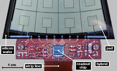
"Pad hybrid design."
|
Every detector module consists of a silicon sensor (32
pads on a common substrate) and a small printed circuit
board (hybrid) with the readout chip. The hybrid contains
a number of capacitive filters for the ASIC supply voltages
and RC-filters for the threshold and depletion voltages.
There were some capacitors on the hybrid prototype foreseen
to stabilize the chip bias voltages. In the final design
these components were omitted without degrading the chip
performance. The trigger pulse width was reduced from 80 ns
to 50 ns with an external resistor, drawing an additional
bias current.
The calibration circuitry provides a double MIP signal
for the test input of the readout chip. This signal is a short
current pulse generated on the motherboard and transmitted to
the hybrid via the stripline. The pulse is terminated on the
hybrid (to match the characteristic impedance of the stripline),
converted to the voltage, attenuated and transformed into the
charge.
The hybrid circuit diagram and the board layout were created
in the "OrCad" v.9.1 development system. All hybrids passed
electrical tests before and after the ASIC mounting and after
the silicon sensor assembly.