stable if all chips on top side powered
stable if all chips on bottom side powered
stable if 8 chips in centre powered
almost stable if any five chips either side of centre are powered
oscillates if 6 chips powered on left or right side with no chips on
other side of centre.
This implies that: the supply input point has a low enough impedance
to isolate the two halves of the module to some degree
This is perhaps not so suprising since the supply is necked down to
narrow traces in the centre and the 470nF main decoupling cap is directly
across the supply before it fans out.
Question - if these two halves are so isolated then does this explain
why some modules oscillate only when a detector is connected,
the two halves then being joined by a common feedback path via
the detector ?
Power supply observations: We spent some time trying to look at the vcc and vdd supplies.
The first step was to simply clip a scope probe on to the supplies and put the probe ground on to a small piece of wire soldered onto the bottom end of the 470nF decoupling capacitor in the centre of the hybrid . All you can see is a LOT of noise. Averaging is of little use as the main pickup is mainly from the clock and data at a very high level
Clearly the ground was not good enough even though the ground lead was
only a few centimetres long. (if you put the probe tip
on the ground lead you still saw the same noise). We made a small clip
from a strip of brass wrapped around the probe ground sleeve and cut it
to form a tip which allowed the probe to then clip directly across the
capacitors on the hybrid. Now it was possible to observe the power lines
.
So far we have not observed any significant signals across VCC and analog
ground..
The Vdd line is a very different story. Here we see a number of effects
which are significant.
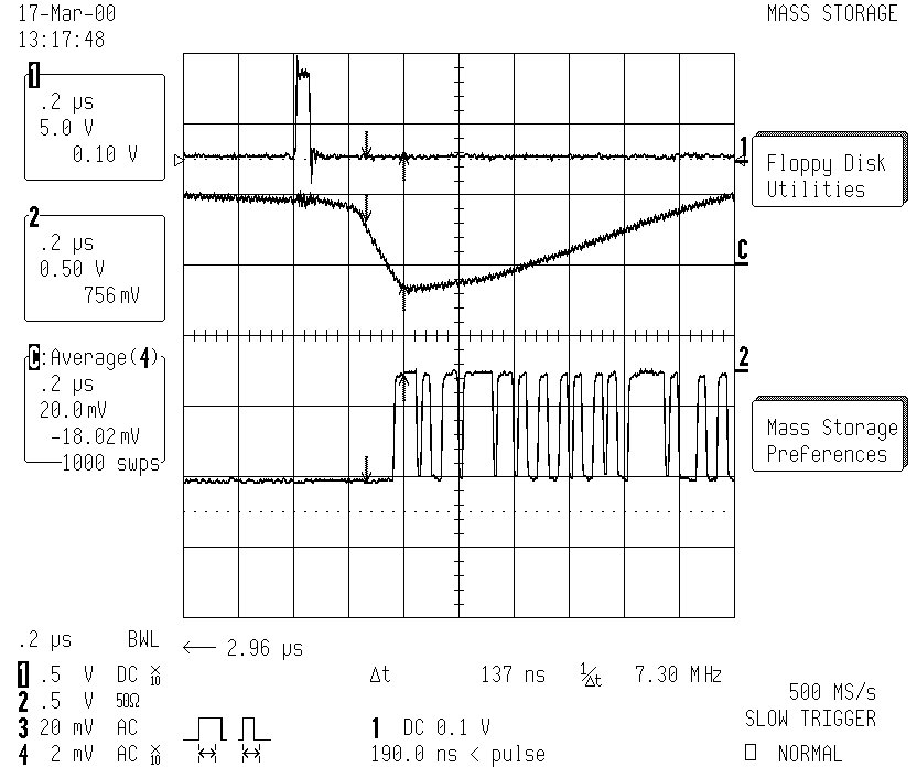
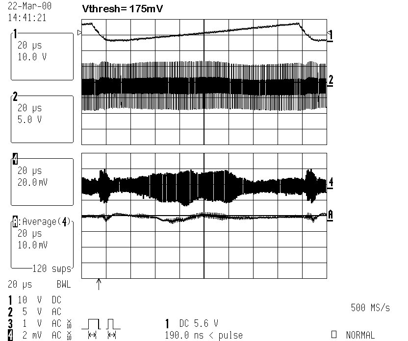
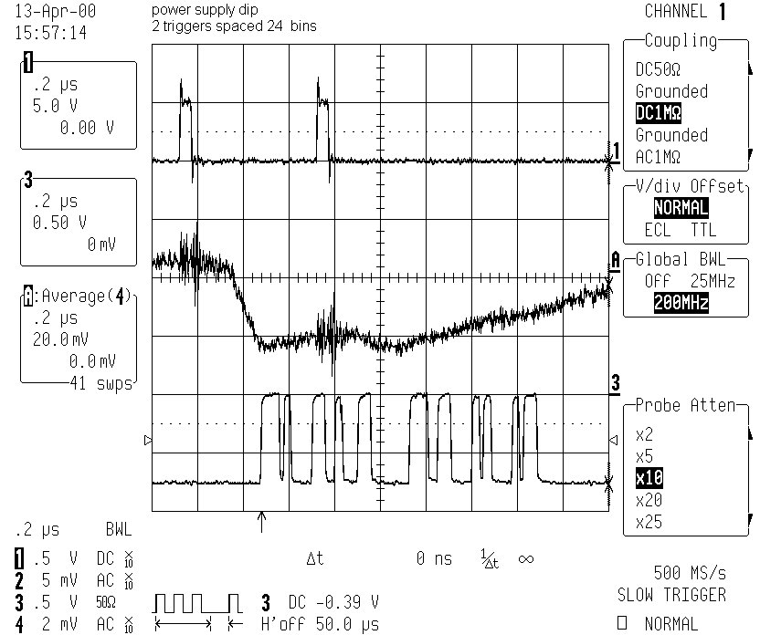
The first is shown below, This is a fast 25mV/125ns transition
on the vdd line just after a trigger and before the readout starts.
There are other dips as the chip is set up but whilst they are
of similar magnitude, the fall time is greater and they would not be present
during data taking.
TRACE 1 shows trigger
TRACE 2 (bottom) shows output data
TRACE C shows averaged VDD power supply voltage
I believe this could cause problems in the system as this is a high speed edge with a low source impedance which is almost impossible to bypass or filter and it will appear on all the outgoing cables from every module just after a trigger . This could create problems in several ways, direct capacitive injection into the overlying strips, injection into the analog supplies or other signals in the stacked power tapes, and create RF emissions outside the tracker which could interfere with other equipment.
Do we know the reason for this current draw at this time? and is it possible to do anything about it in the chip design?? One thought I had was that we could put power line filters on the hybrid using four terminal capacitors ( essentially a surface mount feedthrough) but I am not sure they could do much about this kind of spike because of the low source impedance
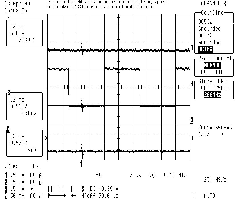
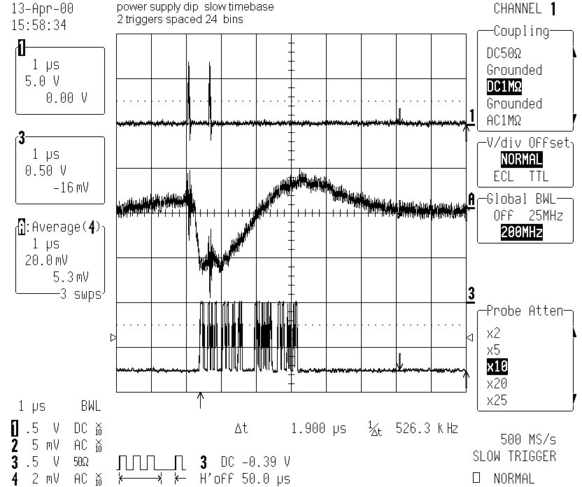
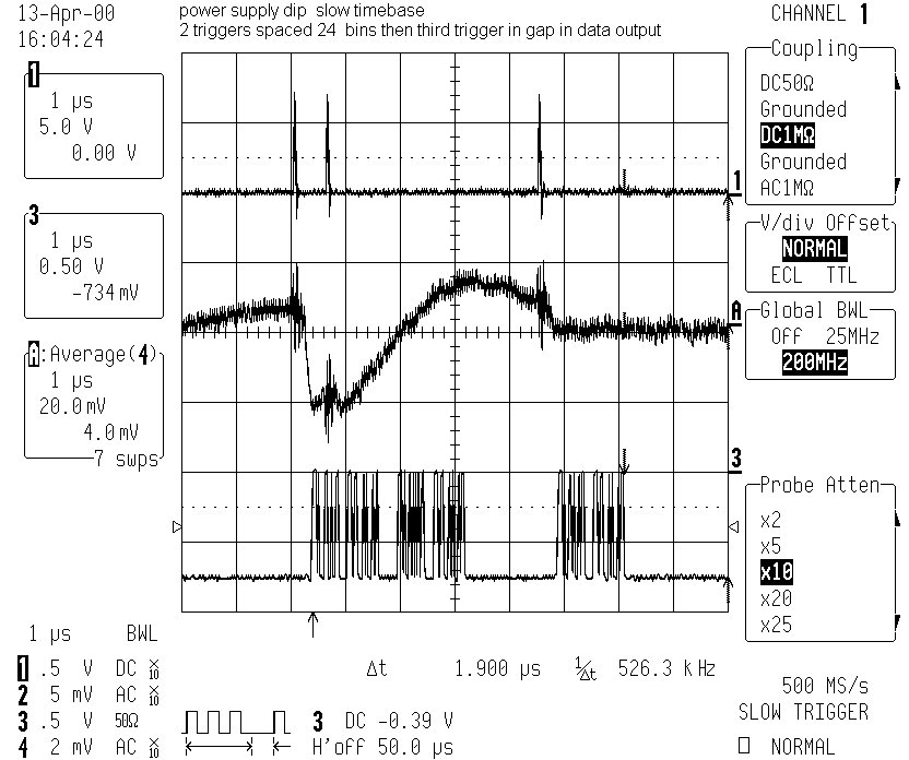
Additional multi trigger traces: note probe
compensation
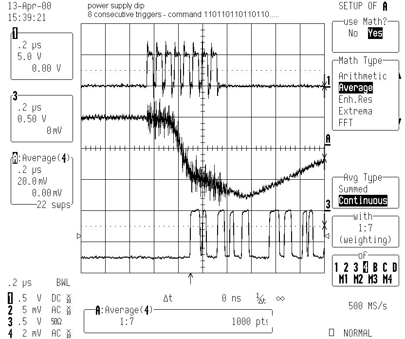
8 consecutive triggers
8triggers with 6bin spacing
8 triggers 6bin spacing - slower timebase
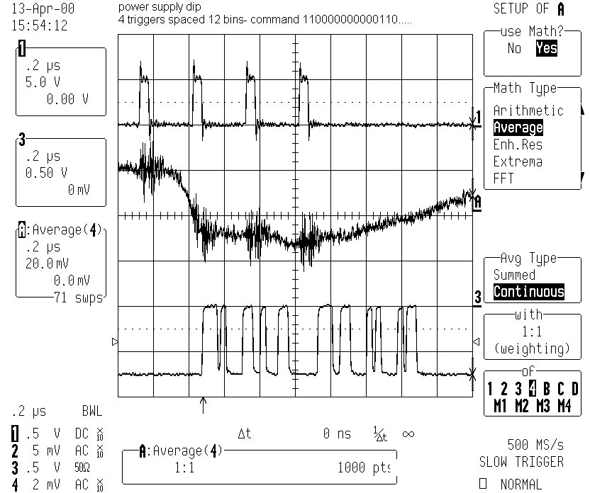
4 triggers 12 bin spacing
2 triggers 12 bin spacing 2
triggers slow timebase 3 triggers
one in middle of data output
3 triggers one after end of first data
3 triggers last one much delayed
The decoupling on Fdd on this hybrid uses an AVX
0.1uf 0603 16v X7R cap at each chip pair plus 1 (7 total) plus an AVX 470nF
0805 X7R
at the power entry ( we did our measurements across this cap). Given
the total capacitance on the hybrid is of the order of 1.2uF( there is
no large tantalum capacitor on the hybrid because I do not believe we should
use these as they fail short circuit - 10uf was tried and made no great
difference) the current pulse here calculates to be (i=CV/t = 1.2e-6 *
25e-3 / 1.25e-7) 240mA or roughly 20mA per chip . This would be
a huge current pulse so I was inclined to think that there is another effect
here which means we are being fooled about its value.
Looking at manufacturers (AVX - go to page 9) data there is no information on the self resonance for these particular caps but a 0.1uf 0805 cap shows a self resonance between 10 and 20 MHz so the 0.47 cap can be expected to have a somewhat lower frequency - the effective series resistance at the resonance can be as low as 0.1 ohms.
I thought it would be interesting to examine the impedance versus
frequency behaviour of the hybrid to see if there were any resonances
and to give some idea of the decoupling effectiveness of the hybrid, chips
and power supply as a system
To do this we used a Tektronics FG504 40MHz function generator.. A
14Vp-p sinewave was injected via a 470 ohm resistor across the digital
supply. Between 10KHz and 8Mhz the signal on the supply was around
18mV p-p - calculating the impedance of the supply this then ccmes to (470
* 18e-3/ 14=) 0.6 ohms in this bandwidth. However between 8 and 27 MHz
two broad resonances were apparent, see below
Notes
1) This is at a high threshold
2) We did try putting additional capacitance across the supply in the
form of tantalums and ceramics but with very little effect. presumably
the series inductance of the additional capacitor connections was too high
to have much effect on lowering the impedance.
3) No significant change to this trace occurred if the support card
supply was turned off i.e. - no clocks applied
4) sweep generator is asynchronous to system clock
5) swept signal does not have constant phase with scope trigger so
we are not fooled by aliasing - this also alows averaging to zero of the
injected signal and leaves the true trace of the power supply dip
6) putting a ferrite around the supply leads as a common mode choke
or around a single lead does not change the picture
>>>> this is a real effect.caused
by the combination of the hybrid traces and decoupling components
.
The Q is low at around 2
: >>>>
Hybrids exhibit frequency dependent characteristics
Questions: does this matter ? What do other hybrids look like ? would adding lower value decoupling capacitors with higher self resonant frequencies help? Is trace inductance/resistance the limiting factor in the supply impedance? Would it be a good idea to scan all hybrids to look for resonances as part of the standard testing??
The above is interesting but it is not clear what it tells us unless we see oscillatory effects at the resonances. .
MORE interesting things at low thresholds - a case for two oscillatory loops including the comparators with and without the amp/shaper and the digital supply
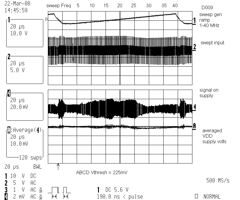
A second interesting effect we have observed is that the digital supply
voltage dips at around 12.5MHz as we sweep the injected frequency (remember
we inject this across the vdd supply) but only when the chips are at low
threshold below the point where they oscillate when we turn on the front
ends of all the chips. The procedure was to set the threshold then to leave
the command line quiescent and make the measurements The next few plots
show how the amplitude of the supply dip increases with increasing threshold
- note that this implies that the current in the VDD line increases with
threshold
If we put the signal generator at a fixed frequency of 12.5 MHz the
supply current does increase - from around 600 to 800mV
Power dips on VDD as frequency injected is scanned for incresing
thresholds - see previous trace for trace identification
linear sweep 1-40MHz approx
5Mhz per division with 20MHz at the centre
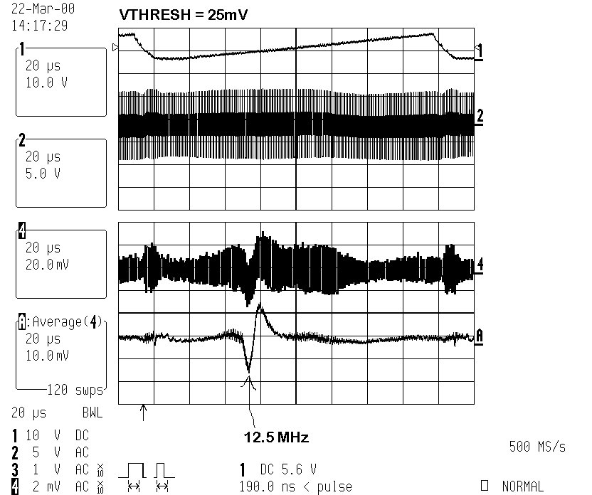
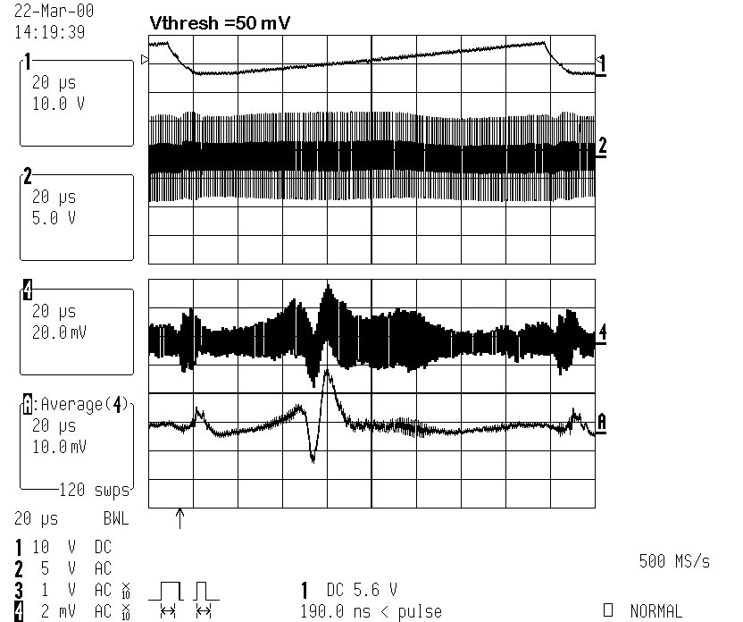
Notes 1) - top trace is frequency generator ramp second trace
is stimulating input before 470 ohms trace 4 is signal on supply
trace A is averaged signal on supply
2) Amplitude
of dip in DIGITAL supply is dependent on number of chips with ANALOG front
ends turned on
3) increasing
amplitude of dip corresponds to increase in supply current
4) Power dip
increases with threshold up to a maximum around the threshold where the
hybrid normally becomes stab;e
5) power dip
is not present at high threshold
Questions - does the incresed power draw occur due to the
comparator switching - if so then can we reasonably infer that as the threshold
increases then the amplitude of the oscillation of the comparator increases
and more current is drawn??
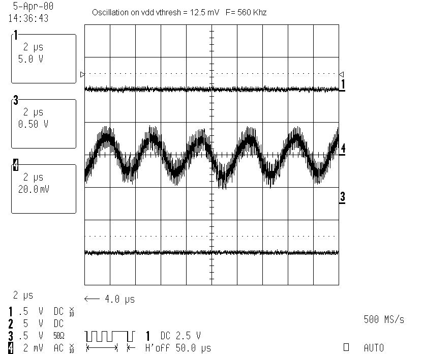
A further observation
Having convinced ourselves that we could see real effects we decided
to look at the digital supply without any stimulation to see if
there was evidence on the power supplies of oscillation at low thresholds
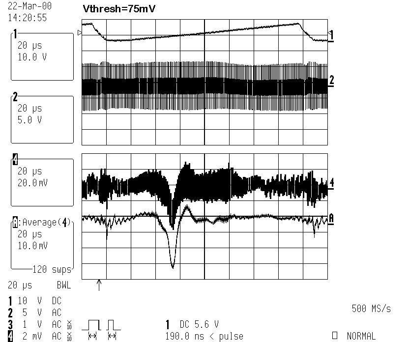
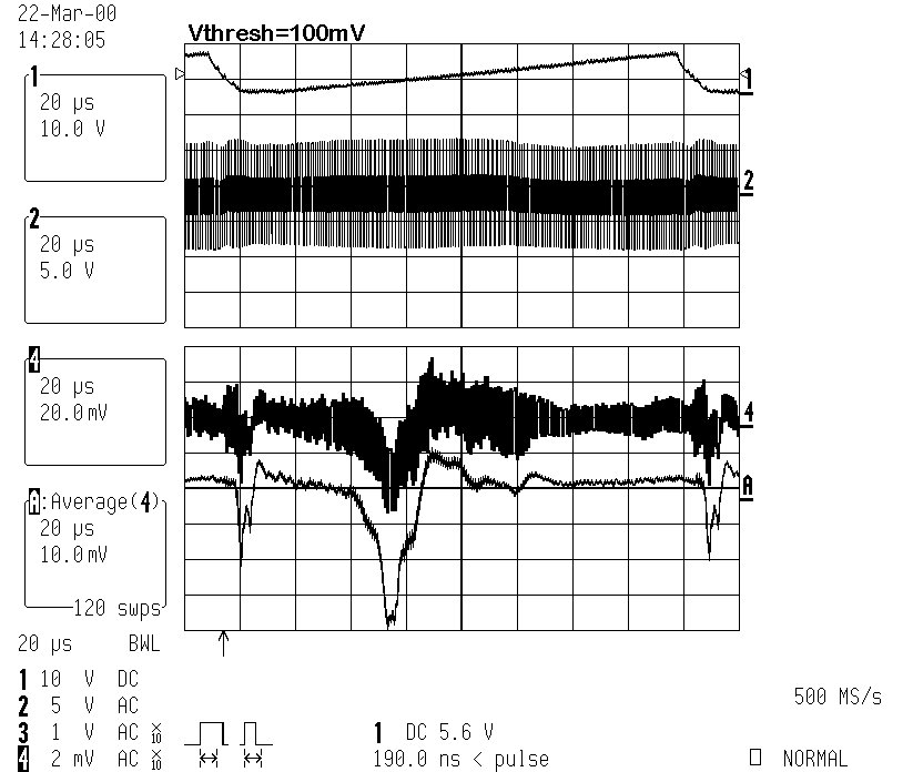
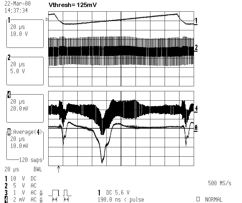
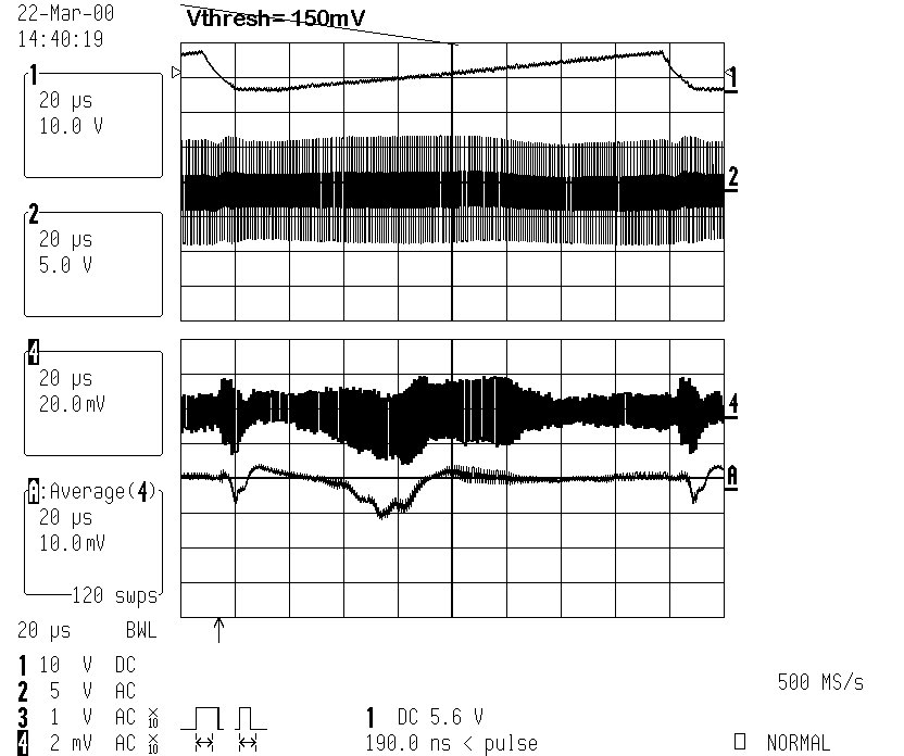
Again the analog supply is relatively quiet. but we do see low frequency
oscillatory behaviour on the VDD supply at low thresholds .(below Vthresh
=100mV
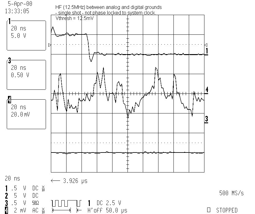
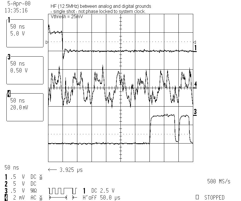
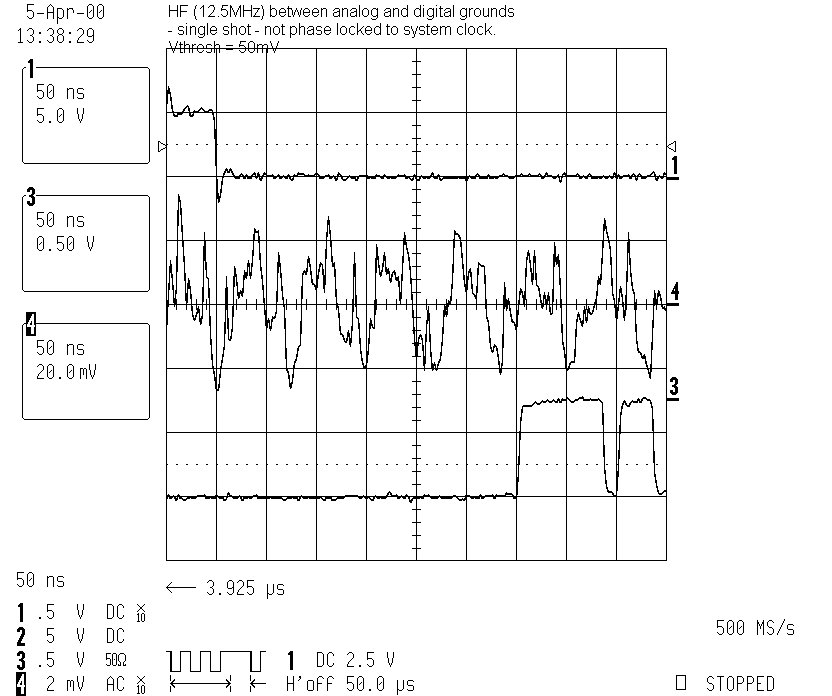
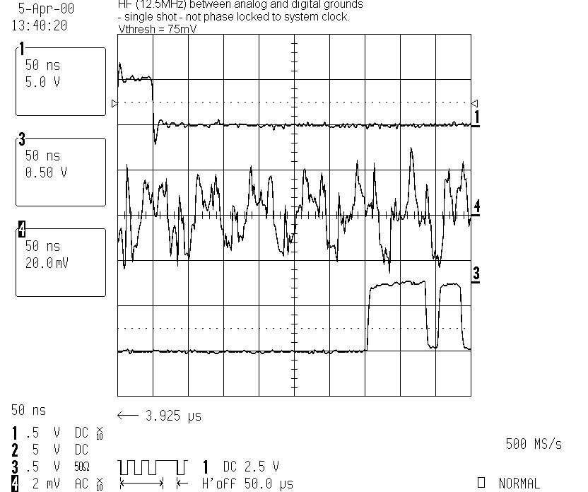
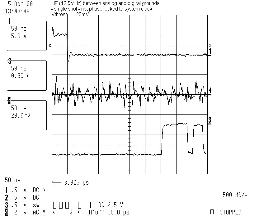
At the same time we also see a 12.5MHz oscillation measured between
the analog ground and digital ground at the end of the hybrid furthest
from the power connector.. It does not appear to be phase locked to the
system clock.
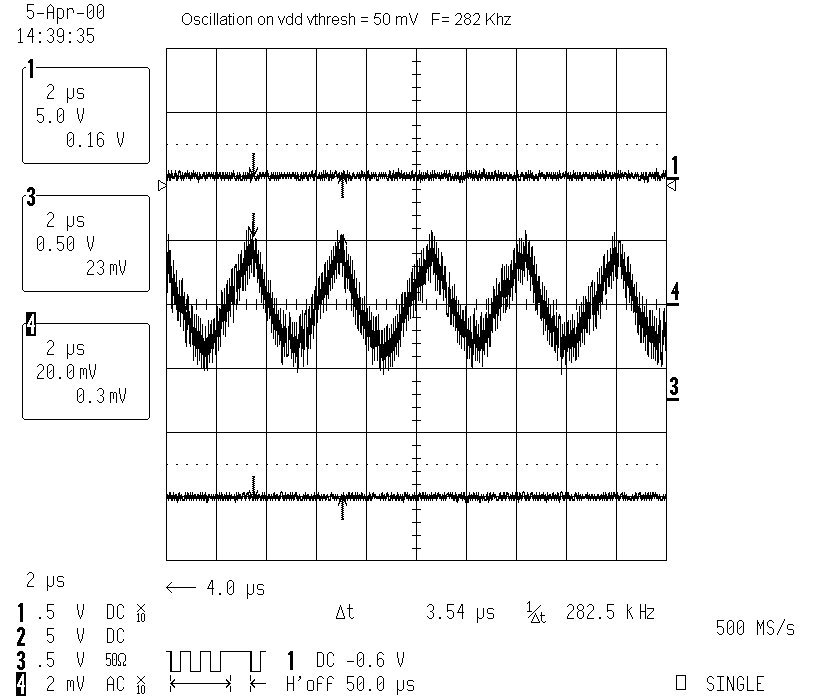
The low frequency oscillation we see across the Vdd is dependent on
vthresh but is in no way linear. The frequency seems to jump between
different discrete values, it varies from being almost sinusoidal to a
series of cusps. to a sawtooth. The amplitude can be up to 30mV.
Sometimes there are multiple frequencies which are not phase locked to
each other.
occupancy plot with no calibrate
.pdf. all 12 chips powered
occupancy ploy with 2fC calibrate
.pdf all 12 chips powered
the table below shows the behaviour we observe - the digital supply
current is shown together with the difference in current relative to the
current at the first stable threshold - Clearly this extra current
is due to one or other or both of the oscillations.
| Vthresh (mV) | IVcc(mA) | IVdd(mA) / delta relative to stability point | frequency on Vdd (KHz) | amplitude across Vdd (mV) | scope plot of Vdd | 12.5 MHz 40mV between grounds | |
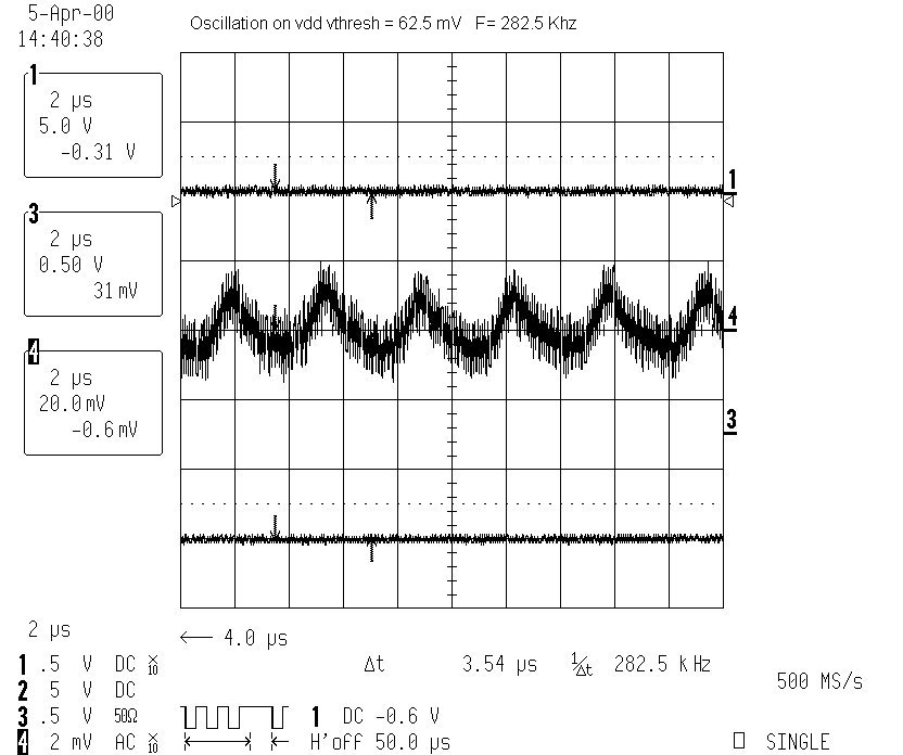
| 12.5 | 880 | 760 +174 | 560 | 20 | vt12mv.jpg | YES | |
| 25 | 882 | 773 +187 | 562 | 20 | YES | ||
| 37.5 | 884 | 779 +193 | 280/620 | 20 | YES | ||
| 50 | 887 | 787 +201 | 282 | 30 | vt50mV.jpg | YES | |
| 62.5 | 891 | 766 +180 | 282 | 20 | vt62mv.jpg | YES | |
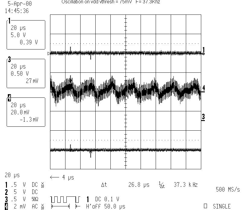
| 75 | 896 | 738 +152 | 37.5/290/2100 | 10 | vt75.jpg | YES | |
| 87.5 | 902 | 690 +104 | 289 | 10 | <10mV | ||
| 100 | 909 | 642 +56 | chaotic | <10mV | NO | ||
| ********* | ********* | occupancy | plot stable | after this | point | ******** | ********* |
| 112.5 | 916 | 586 0 | chaotic | <10mV | NO | ||
| 125 | 920 | 577 -9 | stable | NO | |||
| 137.5 | 923 | 571 -15 | NO | ||||
| 150 | 926 | 563 -23 | NO | ||||
| 162.5 | no data | 557 -29 | NO | ||||
| 175 | 930 | 551 -35 |
The next step is to add links between the analog and digital grounds
to achieve more stability and then to examine the supplies again.
not done yet
A Personal (TS) preliminary interpretation
When oscillation at low thresholds is present then there is an observable
low frequency oscillatory signal across the digital supply.
As the threshold changes the character of the oscillation changes.
Self oscillation of the module is dependent on the number and position
of the chips which have analog font ends switched on. Chips on a common
arm of the supply are less closely coupled to those on another arm
(does this explain the occasional presence of two independent frequencies
when low frequency oscillation is observed?)
>>> the digital supply is involved in the oscillatory loop at low thresholds.
The low frequency oscillation varies from 2.1MHz down to 200KHz - well
below the bandpass of the shaper.
>>>>> the shaper is not involved in the low frequency oscillatory
loop,
DC power in the VDD line increses if the module is forced into HF oscillation.
Stimulated power supply current draw at 12MHz correlates well with increasing
threshold up to the point where the threshold is high enough to stop oscillation
in the unstimulated condition.
>>>>> The energy in both the HF and LF oscillation is provided by the
DIGITAL supply >>>>> the comparators are oscillating in harmony
NOTE - The above does not directly explain why previously stable hybrids
with massive groundplanes can beoime unstable when a detector is
added - perhaps this is driven by the 12.5MHz oscillation with a different
feedback loop via the amp/shaper and this is driven by oscillatary current
flow in the digital power line causing a voltage drop in the commoned
ground??
What can be done????
1) reduce the source impedance of the supply so that the
loop gain is reduced - (remember we already have a measured 0.6Ohm source
impedance in this setup which is pretty low already).
This cannot be done at the supply source in the experiment as we
have long cables and it would not work at high frequencies anyway
We could try decoupling the digital supply more heavily on the hybrid.
. For the low frequency oscillation this may help but the most likely
effect is that we will simply lower the frequency at which the module oscillates.
this is particularly likely if the shaper is not in the loop because there
is no frequency dependent term in the gain loop.. It is also not a good
solution as we are limited in the type of capacitors we can use - essentially
in this environment we can only use X7R dielectric ceramics so even a few
microfarads requires massive components. (N.B. Tantalum caps fail short
circuit - we should not use them)
Utilising smaller capacitance decoupling caps at each chip in parallel
with the existing 0.1uF components is also unlikely to be of much benefit
for the oscillation seen at 12.5 Mhz as the trace inductances will most
likely set the limit for the impedance rather than the intrinsic component
inductance. This of course would not help at all at low frequencies
.
Experimentally tt seems that paralleling the analog and digital grounds
and lower resistance traces are beneficial in reducing the oscillation
down to the 0.3fC threshold. on some hybrids and perhaps eliminating it
entirely on others.
Given the observations above which I believe demonstrate that there
are two oscillatory loops operatiing and that the power to fuel the oscillation
appears to come from the digital supply,then it would seem entirely wrong
to deliberately couple the analog and digital ground returns in a common
impedance. It may be that the coupling that is introduced by doing this
is beneficial for either or both of the high and low frequency loops in
that it adds an antiphase signal in some way, but given the complexity
of the phenomena I do not believe that this is a correct solution as it
is impossible to be sure of the mechanism. The
biggest problem with the heavy common ground plane approach is that, it
is impossible to be confident that we have sufficient margin of stability
that we can build many modules that do not oscillate. If, the comparator
is in the loop then the gain of this is an uncontrolled parameter across
production batches, or even from wafer to wafer. .
2) A quick and dirty fix with a 0.1uF capacitor between Vcc
and Vdd
Before this investigation I believed that oscillation was due
to the long tail pair in the comparator being placed between the analog
and digital supplies and drawing current from one or the other as the comparator
flipped, and so changing the voltage on the analog supply.and completing
an oscillatory loop via the amplifier/shaper . With the shaper in the loop
the oscillation would be in the shaper bandpass and could explain
the 12.5MHz signal seen between the grounds The low frequency outside the
shaper passband would seem to eliminate the amp shaper from being in the
feedback path for the low frequency oscillation. with an additional
more straightforward loop formed by the digital supply leg of the comparator
and the capacitors on the digital supply. If it were the case that
the feedback is via the comparator drawing current from Vcc or Vdd and
causing a drop in the supply then the hybrid word be more stable
if Vdd and Vcc were decoupled with a capacitor. If the current draw on
vdd falls and that on Vcc rises the capacitor holds the voltages constant.
This does indeed make this hybrid more stable . .
can someone try it on a full module???????? .
.
Why is it undesirable to do this in the experiment?? --
because switching noise on Vdd will be coupled into the analog supply-
remember the big dip we see after the trigger!
3) I
beliene the correct approach would be to redesign the chip so that the
comparator is insensitive to the VDD supply (tie both legs of the comparator
to the same supply !!)and use segregated ground planes joined at only one
point to avoid common impedance coupling
I realise this is an easy statement to make and much less easy to implement!!!
Could we add a small resistor at the top of the resistor which
already exists in the analog leg of the comparator then common all
the nodes between the two resistors on each comparator and take this out
to a decoupling capacitor connected to Vdd ????
.
.
Feedback welcome