sctshld4
SCT Detector shielding and grounding. Tony Smith Jan 00
An investigation of the sensitivity of silicon detectors and front ends to electric and magnetic fields.
Abstract
The Atlas SCT barrel and forward silicon strip detector modules will be mounted on metallic cooling tubes. These tubes together with service cables for the modules will pass close to the strips on the detectors. The detector strips on the outside of the barrel modules and the most forward of the forward wheels will be in close proximity to the overall metallic foil shields around the detector structure. In both the forward and barrel detectors the strips on individual modules will overlap the strips on adjacent modules. Current flow in the tubes or the cables will produce both a magnetic field around the tubes and cables, and a voltage drop along the tubes and cables. The magnetic field produced will impinge on the modules and produce a noise signal in the input circuit loop. Voltage drops along the tubes, the cables and the screens will be applied to the detector strips across the parasitic capacitances between modules and the structure and between any modules with overlapping strips, also generating a noise signal in the input circuit. This document attempts to quantify the relative levels of susceptibility of the module to the effect of current flow in the tubes, cables and foil screens in order to allow decisions to be made on the grounding and shielding architecture that should be adopted in the barrel and forward SCT detectors.
In the SCT Barrel and forward detectors there are several identifiable positions where detector strips could be exposed to electric and magnetic fields due to current flow in cables screens and the foil screen of the envelope.
For electric fields these are:
a) Barrel detector strips overlapping neighbouring strips or hybrids or pipe work 12 cm along the axis of the strips and separation of 1 cm ? (~10 fF, Noise voltage required for 100 electron noise increase above 1500e- ~ = 8.25 mV)
b) Barrel detector strips overlapping neighbouring modules on the same stave 0.2 cm long separation 0.3 cm. ( ~0.5 fF, Noise voltage required for 100 electron noise increase above 1500e- ~ = 180 mV)
c) Barrel detector strips on the outer layer next to the outer foil shield 12 cm along the axis of the strips and separation of 1 cm ? (~10 fF, Noise voltage required for 100 electron noise increase above 1500e- ~ = 8.25 mV)
d) Forward detector strips to strips on an adjacent module 12 cm long and separation of 0.3 cm (~35 fF, Noise voltage required for 100 electron noise increase above 1500e- ~ = 2.5 mV)
e) Forward detector strips overlying cooling tubes under the module with a worst case estimate of 12 cm long and separation of 0.3 cm where tubes exit from the disk radially (35 fF, Noise voltage required for 100 electron noise increase above 1500e- ~ = 2.5 mV)
f) Forward modules in the most forward disk where strips are facing the foil screen at the end of the forward cylinder 12 cm long and separation of 0.3 cm ?
(~35 fF, Noise voltage required for 100 electron noise increase above 1500e- ~ = 2.5 mV)
For magnetic fields these are:
a) Barrel detector strips parallel and closest to cooling tubes, cables and screening foils 12 cm long with a loop height of 0.03 cm 1 cm below strips
strip loops virtually immune because of symmetry – pickup only into backplane loop. estimate?
b) Forward modules where supply tapes pass underneath and parallel to the radial strips with a separation of 0.7 cm over 12 cm.
c) Forward modules where cooling tubes pass underneath and parallel to the radial strips with a separation of 0.3 cm over 12 cm. where tubes exit from the disk radially
In addition to the input loop area formed by the strip and backplane an additional loop area, which is susceptible to magnetic fields is encompassed by the connections to the backplane decoupling capacitor, the coupling here is dependent on the hybrid circuit layout and implementation of the backplane connections.
For the electric field case it is relatively simple to calculate the parallel plate capacitance and the charge coupled into a strip for a given voltage step.
The magnetic field case is not so simple. The coupling is dependent on the field geometry and the angle at which the field cuts the input loop. In addition the field produces a noise voltage in series with the input so it is necessary to know the impedances in the input loop to determine the magnitude of the noise current, which will be injected into the input.
Electric field coupling
Silicon strip detectors are particularly sensitive to changes in electric fields due to their charge sensitive front ends and large area strips, which can have significant parasitic capacitive coupling to conductors or other detectors.
Example calculation for order of magnitude of the effects
Take a simple case of two modules overlapping along the full length of 12 cm with a 3 mm gap between the strips on one module and the strips on another module. as in the forward region.
The amplifier inputs are virtual earths so the strips on each detector will be forced to the AC potential of the amplifier ground reference point on each of the modules. Therefore any potential difference between the ground reference points on the two modules will appear as a potential difference between the two silicon detector faces. From the point of view of a single strip on one of the detectors in the overlap region, the opposing face of the superposed detector will appear as an equipotential second plate of a parallel plate capacitor with a capacitance determined by the area of the strip and the separation of the strip and plate.
For a 12 cm strip of width 100 um (assume all field lines in the width of one strip pitch terminate on the strip) and separated by 3 mm from the overlying detector then:
C = 12e-2 * 1.0e-4 * 8.85e-12
------------------------------------ = 35.4 fF
3e-3
This parasitic capacitance is connected directly to the input of the strip amplifier
and consequently any voltage change across it will inject a signal in the same way as the on chip calibrate capacitor is used to inject a known calibration charge.
What size of signal
would we need to add to see a 100 electron increase in the noise?
Assuming the baseline noise in SCT modules from multiple sources is around 1500 electrons then if a further uncorrelated noise signal is injected via the parasitic capacitance to a plate it will add in quadrature to the pre existing noise.
Noise total = sqrt (Noise initial**2 + Noise added**2)
Rearranging, Noise added = sqrt(noise total**2 - Noise initial) = sqrt (1600**2 – 1500**2) = 557 electrons RMS
The RMS noise voltage required across this parasitic capacitance to increase the noise by 100 electrons
= 557 * 1.6 e-19
------------------------ = 2.5mV
3.54e-14
.
If the injected noise is doubled to 1114 electrons the total noise increase seen is almost fourfold to 400 electrons.
Induced noise current in electrons 0 557 800 995 1166 1322
Factor relative to 100 electrons 0 1 1.44 1.79 2.09 2.37
To give total noise of 1500 1600 1700 1800 1900 2000
An increase of 0 100 200 300 400 500
>>> extra noise increases almost as the square of the culprit signal. Clearly the onset of any effect will be sudden and increase rapidly.
Suggested practical test of sensitivity of modules to capacitively coupled noise
If a foil is placed over a detector and driven with a sinusoidal signal at different frequencies and amplitudes it should be possible to plot the sensitivity of the front end to electric field pickup.
Method
Place a detector in a metal framed box with a plastic window made of a material with a known Er and place a foil over the window The foil should be isolated from the rest of the metal frame. A coax cable from a signal generator should have its screen taken to the module ground point and the inner of the coax should be taken to the foil and then to the module ground point via a 50 ohm resistor. The capacitance to the strips can be calculated once the height to the window and the thickness of the window are known.
From this the sensitivity per fF per volt RMS versus frequency can be plotted for a few values of excess noise.
Magnetic field susceptibility of the detector and front end
The front ends of Silicon strip detector modules are susceptible magnetic fields in their passband due to the loop area encompassed by the strip, the backplane metallisation, the fanin structure and the chip input and reference (analog power ground) connection. Magnetic fields can also couple into the loop formed by the conductors connecting the backplane decoupling capacitor, through the strip to backplane capacitance (many in parallel), the amplifier inputs, the amplifier reference (analog ground) and back to the decoupling capacitor.
Depending on the angle of incidence of the magnetic field there are a number of identifiable loops. Any magnetic coupling into these loops will generate a noise voltage in the loop, and hence a current determined by the loop impedance. The coupling is directly proportional to frequency, current in the offending conductor, inversely proportional to the distance from the culprit conductor and proportional to the cosine of the angle of incidence.
Let us examine the six cases of a magnetic field cutting the detector, these are
a) A culprit radiating wire parallel to the strips and above or below the detector
b) A culprit radiating wire parallel to the strips in line with the detector plane at either side of the detector
c) A culprit radiating wire orthogonal to the strips and above or below the detector
d) A culprit radiating wire orthogonal to the strips and in the detector plane at either end of the detector
e) A culprit radiating wire normal to the detector plane and centrally at the side of the strips
f) A culprit radiating wire normal to the detector plane and at the end of the strips
For the above cases there are different coupling loops formed by the strips and backplane, between strips and any loop area enclosed by traces to the backplane decoupling capacitor and from the capacitor back to the amplifier ground.
Cases a) and b) are clearly the worst cases for loops where the strips and backplane form the greater part of the loop.
They also cut any loop in the backplane decoupling capacitor traces.
These cover the case of pipe work or cabling in the barrel and some of the pipe work and cabling in the forward
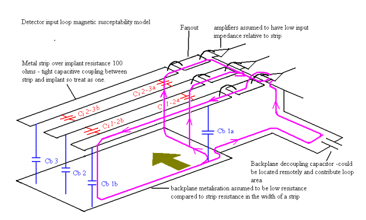
Figure 1
Cases c) and d) do not contribute any coupling to loops formed by the strips and backplane as the field is in the plane of the loop
They do couple into loops formed between adjacent strips, the inter-strip capacitance, and the amplifiers. For strips in the centre of the detector the opposing current in the neighbouring strip will cancel the effect. For strips at the edge the compensation is not balanced and some net effect may be seen. They also couple into any loop formed by the decoupling capacitor traces. These cover the case of some parts of the pipe work and cabling in the forward detectors.
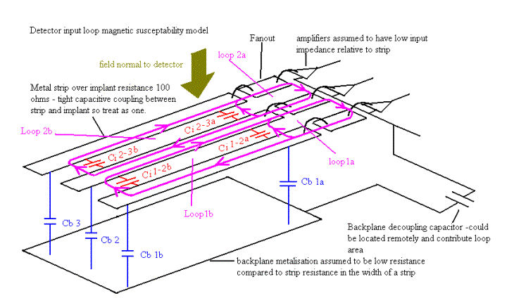
Figure 2
Case e) Field lines cut the strip and backplane loop tin both directions so the net flux is zero in the strip and backplane loop. There will be no contribution to a loop formed by connections to the decoupling capacitor, as these traces will be in the same plane as the field.
Case f) The field lines cut the strip backplane loop and will couple into it but the field is decreasing by 1/r along the length of the loop
Again, There will be no contribution to a loop formed by connections to the decoupling capacitor, as these traces will be in the same plane as the field.
From the above it can be seen that:
1) The largest coupling to the strip backplane loop will be from a current carrying conductor running parallel to and above or below the strips
2) Any loop formed by the conductors to the backplane decoupling capacitor can couple signals into the input loop.
How will the coupling influence the input circuit
A sinusoidally varying magnetic field B with constant field intensity cutting a loop area A at an angle theta will induce in the loop a voltage equal to jw B A cos theta.
In the case of a strip and backplane loop with a low impedance amplifier at one end, then the loop is closed via the strip to backplane capacitance, Csb. If we assume that Csb is the dominant impedance in the loop relative to the strip resistance or the amplifier input impedance then we can consider the strip and backplane to be shorted at the amplifier input and Vsb to be close to zero. The voltage in the loop will be induced incrementally along the length of the strip and backplane conductors so at the far end of the strip the maximum voltage difference will occur. This means that the voltage across the distributed Csb will increase linearly with distance from the amplifier from zero to Vsb max so the average voltage across Csb will be Vsbmax / 2. Alternatively one can think of the effective capacitance being halved or the impedance of the capacitance being doubled. Having determined the impedance of the loop as 2 * Xcsb it is now possible to calculate the current in the loop and the signal seen by the amplifier.
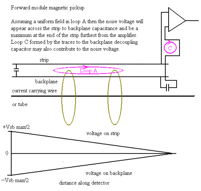
Noise voltage distribution along strip and backplane for forward configuration
Differences
between barrel and forward detectors with respect to electromagnetic coupling
Figures 1 and 2 essentially represent the geometry of a forward module with amplifiers placed at the ends of the strips. In a barrel module the amplifiers are placed at the centre of the strips and the loop geometry is rather different. Here the strip and backplane loop is essentially split into two halves with the amplifier at the centre. Now we have a balanced situation where Vsb max occurs at one end of the strip and –Vsb max at the other end and the current induced at the amplifier from one half of the detector is exactly matched by an equal and opposite sense current from the other half of the detector.
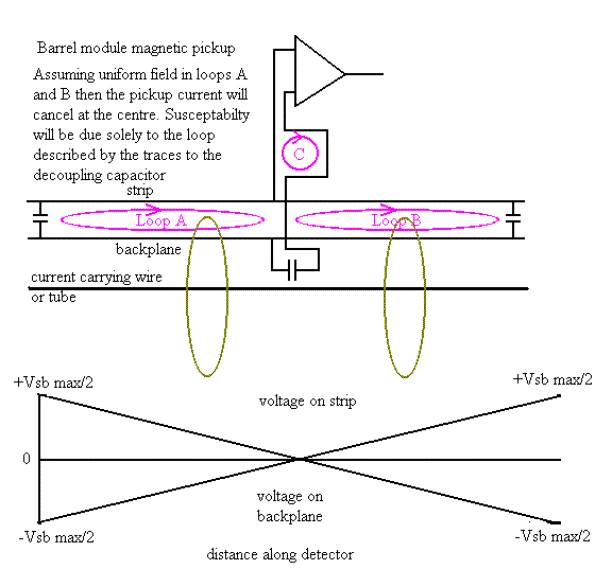
Noise voltage distribution along strip and backplane for barrel configuration
Clearly in the case of the barrel, to first order, there will be no net susceptibility in the strip backplane loop to magnetic fields from current flowing in a conductor parallel to the strips, such as the cooling tube or power cables. Any magnetic pickup seen is likely to be due to second order effect such as non uniformities in the field or from coupling into the loop formed by the traces to the backplane decoupling capacitor ..
. Conversion of magnetic field induced voltages to electrostatic pickup, ---- is this a problem?
Even if the currents are essentially balanced it can be seen that a voltage gradient exists along the strip. If these potentials are sufficiently large then it is possible that the parasitic capacitance of the strip to a shield or to another module will induce a signal into the input. For this to be significant the stray capacitance would need to be of the same order of magnitude as the strip to backplane capacitance of 2.4 pF . A calculation shows that the capacitance of a 12cm strip to a plate 3 mm above the strip is of the order of 35 fF which is almost a factor of 100 down and we can neglect the effect
Example calculation for order of magnitude of the effects in the strip backplane loop
Let us take the loop area enclosed by a 12 cm strip and its backplane on a 300 um thick detector as an example and calculate the current required to flow in a single wire spaced 1 cm from the loop to generate a 10 MHz sinusoidal signal of an amplitude equal to that necessary to give a 100 electron increase in noise at the amplifier above an assumed initial level of 1500 electrons
The loop impedance will determine the current generated in the loop by the induced voltage so it is necessary to estimate the impedance. The impedances in the loop are those of the amplifier input impedance, the strip resistance, the backplane resistance, the impedance of the strip to backplane capacitance and the return path from the backplane to the amplifier ground. The issue of the return path is one where there is some debate. Figure 1 shows two possible paths one via the decoupling capacitor and one via the virtual earth inputs of the other strip amplifiers. In the case where a single strip is stimulated by the charge from a single particle it could be argued that the decoupling capacitor and the amplifier inputs are in parallel and there will be current sharing between them in the ratio of their impedances. Here the impinging field influences many strips, so a large number of the amplifier inputs will have their input voltage raised. (For a wire 1 cm above a detector with 640 strips on a 100 micron pitch, taking into account the angle of incidence and the field reduction as the reciprocal of the distance from the wire the net current will be 44% of the current expected from a uniform field.) If we assume that this current flows mainly in the decoupling capacitor then the decoupling capacitor will have a proportionally smaller effect than for a single strip and we can divide its true value by the effective number of strips stimulated. For two back-to-back detectors with 640 strips each the effective number of strips is 44% of 1280 = 572 strips
Loop impedance calculation
Amplifier input impedance – will be complex but assume low resistance at 10 MHz --- say 30 ohms ??
Strip resistance say 100 ohms
Strip to backplane capacitance 0.2 pF / cm * 12 cm 2.4 pF
Effective Csb is half of this due to distributed voltage profile in strip 1.2b pF
Backplane decoupling capacitance (effective) 10 nF / 572 strips 17.5 pF
Csb is the smallest capacitance and will dominate the capacitive impedance – calculating the impedance of 1.2 pF at 10 MHz gives
Xc= 13.2K ohms, this scales with the reciprocal of frequency so at 1MHz it will be 132k ohms and at 100 KHz it will be 1.32 Meg ohms
And this being
the dominant impedance in the loop, most of the induced voltage will appear
between the strip and the backplane.
(Note that the strip to backplane capacitance and the strip resistance are distributed parameters but are lumped in this calculation. If the strip resistance were the dominant impedance then this would need to be accounted for as field lines cutting the loop at the near end to the amplifier would see a lower impedance and produce more current from the induced noise voltage. If the strip to backplane capacitance is dominant as above, then this is not an issue)
Calculate the noise voltage in the loop
Given that the dimensions of the loop are 12 cm by 300 um for the strip and backplane plus a further 1 cm on the fanout
the total loop area is approximately 40 square mm
Current flowing in a circuit produces a magnetic flux f proportional to the current, the constant of proportionality being the inductance L
f = LI
The inductance depends on the geometry and the permittivity of the medium (assumed to be unity here)
If current flow in one circuit produces a flux in a second circuit there is a mutual inductance M 1-2 between the two circuits
M1-2 = f 1-2 / I1 --------1
The noise voltage induced in the second loop is given by:
. . Vn = jw M 1-2 I1 ----------2
We wish now to calculate M for a simple geometry where we have a loop formed by the strip and backplane with constant flux produced by a parallel single wire cutting the loop normally.
The flux density B at a distance r from a current carrying conductor is given by
B = m I /2p r Biot-Savart law --------3
If we assume that
1) The return current flow is in a remote conductor and the field from this does not influence the second loop.
2) That the second loop dimensions are so small such that the flux density is constant across it
3) The field is normal to the loop. (worst case )
4) The strip backplane loop area is A
Then the total flux cutting the loop due to the field around the wire is
f 1-2 = B A cos q Where cos q =1 as the field is normal to the loop
Substituting into 1 for f 1-2 we have
M1-2 = B A cos q / I1
Substituting for B from 3 and cancelling I we have
M1-2 = m A cos q /2p r
The noise voltage in the loop can now be calculated from 1 as
.
Vn = jw
m
A cos q
I1 /2p r
Substituting 2p f for jw and putting in numbers then at 10MHz
Vn = 2p 10 7 4p 10 - 7 40 10 - 6 I1 / 2p 0.01
Vn = 0.05 I1 ------ 4
So for 1 mA of current at 10 MHz in the wire we would expect to see 50 uV at the end of the strip relative to the backplane
If we wish to have a measure of the voltage in the loop with respect to frequency we have
Vn = 5 * 10 -9 f I1 ------- 4a
Thus the noise voltage scales linearly with frequency
Calculate the noise current in the loop
Now the voltage across Csb will determine the current in the loop, this will be
I loop = Vn/ XCsb = Vn * 2pi * f * Csb(effective) = 7.54e-5 Vn
substituting for Vn from 4 we have Iloop = 7.54e-5 * 0.05 * Iwire
Or Iloop = 3.8 e-6 Iwire @ 10MHz ------5
Now we can estimate the effect on the noise of the amplifier of a 10 Mhz sinusoidal current being input to the amplifier
The following is a crude attempt to estimate the effect and is very far from a mathematically sound calculation but hopefully it is within an order of magnitude --- any help would be appreciated!!!!
What size of
signal would we need to add to see a 100 electron increase in the noise?
The measured noise in the system from multiple sources is around 1500 electrons. If we now inject a further uncorrelated noise signal then it will add in quadrature to the pre existing noise.
Noise total = sqrt (Noise initial**2 + Noise added**2)
Rearranging: Noise added = sqrt(noise total**2 - Noise initial**2) = sqrt (1600**2 – 1500**2) = 557 electrons RMS
If we take the peaking time of the shaper (25 nS) as the time over which this signal changes, then the rms current noise would need to be
I=q / t = 557 * 1.6e-19 / 25e-9 = 3.56 nA rms
NOTE – If the injected noise is doubled to 1114 electrons the total noise increase seen is almost fourfold to 400 electrons.
Induced noise current in electrons 0 557 800 995 1166 1322
To give total noise of 1500 1600 1700 1800 1900 2000
So the extra noise increases almost as the square of the culprit signal
Now for the dodgy bit. If we think of a 10 MHz sinewave, which is close to the centre frequency of the shaper it has a 1/f of 100ns so we will need 100/25 times the amplitude to induce the same current variation in the 25 ns shaping time
If this is true then we need approximately 14 nA of current at 10 MHz to see a 100 electron change in the noise
Then what current would we need in the wire suspended 1 cm over the detector?
using equation 5 the current in the wire would need to be Iwire = Iloop/3.8e-6 = 14nA / 3.8e-6 = 3.7 mA at 10 MHz
- Consistency check--- if we know the voltage induced in the loop and the effective capacitance of Csb the we can use Q=CV to calculate the number of electrons flowing in the loop From 4 Vn = 0.05* Iwire
Q = 1.2pF * Vn = 1.2e-12 * 0.05 * 3.7e-3 = 2.2e-16
Dividing Q by the charge on an electron we have N = 2.2e-16 / 1.6 e-19 = 1375 electrons.
This is a factor 2.5 too large - But at least we are not an order of magnitude out!
The above calculation gives some idea of the susceptibility of the strip backplane loop at 10 MHz but what happens at higher and lower frequencies?
From 4a we have Vn = 5 * 10 -9 f I1 and the loop current is determined by the impedance of Csb
Then we have
Iloop = Vn 2p f Csb = 5 * 10 -9 f Iwire 2p f Csb
Substituting for Csb =1.2 pF we have
Iloop = 3.78e-10 f 2 Iwire where f is in MHz
It can be seen that the noise coupled depends on the square of the frequency so combining this with the response of the shaper the rolloff as the frequency decreases is very rapid. For higher frequencies the coupled noise rapidly increases but again the shaper rolls off rapidly above its centre frequency.
(----> need to know how fast it rolls off put in CR-RC response)
I
This would seem to be a quite large effect for quite a small current but it must be remembered that the calculation is done for a single conductor where the return current is flowing in a return conductor, which is remote and does not greatly affect the magnetic field. In practice this will not be the case for power and signal conductors, which will be arranged so that the return current travels in close proximity to the outgoing current and contributes a nearly equal and opposite field.
In this case the coupling will be several orders of magnitude smaller
=====>> Differential mode current noise is a small contributor to pickup.
The exception to this balanced situation with field cancellation is where common mode current flows through power and signal conductors, shielding foils and the cooling tubes
=====>> Common mode current noise is the biggest contributor to pickup..
In the case of the cooling tubes within the shield a net magnetic field will exist if current is allowed to flow through the tubes. This raises the question of trying to demonstrate the effect and deciding if it is likely to be significant in the design of the grounding and shielding scheme for the detector. .
Experimental measurement of magnetic pickup
Barrel system test
In the calculation above the geometry of the strips and amplifier were assumed to be those of the forward modules. However for the barrel geometry it has been argued that because of the low impedance amplifier input being placed at the centre of the strips then there will be cancellation of any induced current, so the module should be relatively immune to pick up from the strip backplane loop. Any remaining sensitivity to current flow in the cooling tube is likely to be due to any loop area enclosed by the connections to the backplane decoupling capacitor.
To test the susceptibility I suggest that a setup be constructed to allow a current to be passed along the cooling tube with the return current part of the loop at a reasonably large distance (say 30 cm) so that it subtracts only a very small fraction from the field generated by the tube. For this test it will be necessary to isolate the tube at one end so that the current cannot flow by any other route than the tube.
Figure 3 shows the principle and geometry of the setup
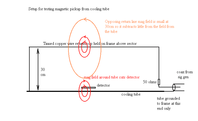
Figure 3
Some problems with this simple arrangement
There are some problems here.
1) The first is that at high frequencies the wire forming the loop will have significant self-inductance so there will be a voltage drop along the tube.
Textbook nomographs for the inductance of straight wires show that the inductance per unit length is a function of total length and no account is made of the fact that here we have a loop. A best estimate from a nomograph shows the inductance of a 2.5mm wire 2.5m long is around 3.5 uH.. The loop here has sides of 1.5m *0.3m so is 3.6m long giving an inductance for the loop of the order of 5 uH giving an inductive reactance of around 315 ohms at 10 MHz. Quadrature addition of this impedance and the 50 ohms gives 319 ohms impedance so to drive 10 mA around the loop at 10 Mhz would need an input signal of 3.19 volts. 3.1volts will appear across the length of the wire so over the 12cm length of the module the voltage drop will be
0.12 m * 3.1v /3.6m = 103mV
The problem now is that we will be applying a significant electric field potential across the stray capacitance from the tube to the strips rather than just a magnetic field to the strips and backplane decoupling capacitor loops
One way of minimising the effect from this would be to tie the module ground to the cooling tube at the centre of the portion of tube adjacent to the module. In theory the potential on the tube relative to the strips will be positive on one half of the module and negative on the other half of the module relative to the central connection to the tube. In practice it is likely that the electric field symmetry will not be perfect so some net coupling will still exist.
2) If the detector is in the centre of the tube, as drawn, then there will also be a voltage drop along the tube between the end of the coax and the module. This distance can be estimated as around 0.7 metres so the voltage drop will be 0.7 * 3.1/3.6 = 603mV
If the module signal ground is connected to the tube either capacitively or directly in order to equalise the potential of the tube and the module then a further problem arises. If the tube is connected to other tubes at the end from which the coax is connected then the other tubes, having no current flow in them will be equipotential at the same voltage as the coax end of the tube the module is mounted on. This potential will then be 603mV different to that of the module ground and electric field coupling will occur across the parasitic capacitance between the adjacent tube and the strips.
To eliminate this coupling it would be necessary to interpose a conductive foil shield tied to the module ground between the module and the offending neighbouring tube
3) The low side of the signal generator output is almost certainly connected to mains ground. The module power leads, although they are not directly connected to the power ground will have a significant capacitance to the power ground. It can be seen that the previously calculated voltage drop of 603 mV between the input signal screen and the point where the module is grounded to the cooling tube will be applied to this loop and this will drive a current around the loop. This will appear as a common mode current in the power supply cable. If there is an imbalance in the capacitance of the cable conductors to the power ground it then it is possible that series noise can be coupled into the power supply or signal lines to the module and this may affect the module noise, contaminating the measurement. This impedance of this parasitic loop will also shunt the inductive reactance of the tube and as the impedance will depend on the capacitance of the cable conductors to mains ground via cable shields or simply to any metalwork then the cable shield configuration will influence the coupling.
A question prompted by the above observations is
What is the relative contribution of the magnetic coupling to that from capacitive coupling due to voltage drop in the tube at 10 MHz and is it sensible to try to separate the two coupling modes. I can clearly be seen that to obtain a current in the tube of a magnitude sufficient to couple to the strips magnetically then there are already very significant voltage drops occurrig in the tube. Scaling calculation in 2 above then approximately 200 mV will exist on a neighbouring tube when the 3.7mA of current required for mag field influence are flowing. With 1cm separation between the strips and the tube giving 10fF capacitance the voltage needed for 100electrons noise increase due to capacitive coupling would be of the order 7.5mV compared to the 200mV calculated signal.
Conclusion – the
magnetic field susceptibility of the strip to backplane loop from current
flowing in the tube, even with ideal mag field geometry, will be a factor of
more than 20 less than that from electric field coupling
For the barrel,
the field cancellation from the central readout will make this factor much
larger and we could safely ignore magnetic field coupling to the strips.
But could coupling to the traces to the backplane
decoupling capacitor still be problematic?
----- calculate area required – field intensity decreases
with distance and neighbouring tube has opposing field.
Given that the calculations have assumed a strip to backplane loop area of 40 sq mm then
Need diagram here to show modified setup using a wire over the module where signal is fed in at the module with coax ground, a foil shield and the wire being tied to the module analog ground.
Method
The setup is constructed as in figure 3. The tinned copper wire loop should be of a substantial cross section (say 16 gauge or larger or possibly made from a self-supporting piece of aluminium angle or tube)
A signal generator is connected via short coax cable. It should be powered, set to 10MHz sinewave and the output voltage set to zero.
A calibration run is now done to establish a baseline noise for the setup.
The output voltage of the signal generator voltage should now be adjusted so that the voltage measured differentially across the 50 ohm load is 0.5 volt, which will drive 10 mA of current around the loop. Note that it is important to measure the size of the signal on each side of the 50 ohm resistor and subtract the two signals because at higher frequencies the inductance of the loop will become significant, and a simple measurement of the generator output voltage will overestimate the current. (Note. I estimate the reactive impedance of this 3 metre loop is around 310 ohms at 10MHz so the voltage required at the signal generator output to provide
0.5 volts across the resistor will be around 3.14v volts Current leads voltage by 90 degrees in the inductance so total drive voltage is the quadrature addition of the voltage across the inductor and the voltage across the resistor)
A noise scan should now be done
Depending on the result of this noise scan, further scans should be taken after adjusting the output level and /or the frequency
I suggest frequency should be scanned in decades from 10KHz to 50MHz in half-decade steps. The output voltage of the generator should be adjusted each time the frequency is changed so there is always the same voltage across the resistor and hence the same current in the loop. If there is a marked peak in the response versus frequency then a finer scan may be useful.
Non-sinusoidal stimulus
It would be interesting to see what the response is with square wave signals and with varying mark space ratios, however it is difficult to see how to interpret the results as the inductance will limit the current of the high frequency components of the signal so the current waveform will not be the same as the applied voltage waveform. This should be evident from the voltage waveform seen across the resistor.
What we might expect to see
The calculation has been done assuming that the magnetic field cuts the loop area of the detector at right angles (cos theta = 1) however in this setup the cooling tube is very nearly in the same plane as the detector so the field will cut at a small angle so the effect will be considerably smaller. The positive side to this is that the angle of incidence will be nearly constant with distance from the tube so, if the effect is measurable, it may be possible to see a difference in the noise on strips depending on the strip proximity to the tube. Note that the 1/r dependence will be convoluted with the quadrature addition of noise so the falloff of noise with distance will be much more rapid than the 1/r relationship alone would give.
Potential inaccuracies
The strips are sensitive to capacitively coupled charge
What if we don’t see an effect (or even if we do).
Should it prove impossible to see an influence on the noise from current in the tube (or even if it is possible) it would be useful to check that it is possible to see the effect from a wire 1cm above the detector, Figure 2 . This would involve almost the same setup except that instead of the cooling tube carrying the loop current, the loop is closed by a tinned copper wire suspended 1cm above the detector and preferably not centrally but offset to one side.
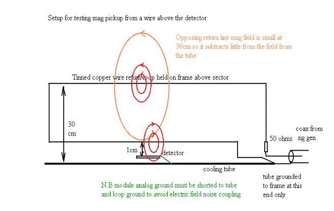
Figure 4
NEED RESULTS HERE TO DRAW CONCLUSIONS
ALSO NEED SETUP WITH OVERALL FOIL SCREEN AND TUBE SHORTED TO IT AT BOTH ENDS TO SEE IF CURRENT IS DIVERTED TO THE SCREEN AND THE EFFECT REDUCES