This page summarises the work done in the silicon detector laboratory of the HEP Group (University of Liverpool - Department of Physics)
|
| Silicon detector studies
This page summarises the work done in the silicon detector laboratory of the HEP Group (University of Liverpool - Department of Physics) |
| The silicon detectors will provide the main tracking capability for the future experiments in high-energy physics. In most of these experiments they will have to withstand a harsh radiation environment. The survival of the detectors to the severe radiation fluences they will receive is a challenge for the detector technology. We are involved in the development of the sensors for several of the major experiments that will take place in CERN-LHC (ATLAS, LHCb) and FERMILAB (CDF). In this page I have collected several results concerning the study of silicon detectors mainly on the subject of their radiation hardness. |
SCT ATLAS sensors page: a systematic study of the radiation behaviors of the sensors for the ATLAS tracker has been
carried out for a few years. The Liverpool University was heavily involved in this program.
A number of results obtained within this program is collected in the following section:
pre and post irradiation characterisation of SCT ATLAS sensors.
Notes
(*) Irradiations were performed in November '98, with the
24 GeV/c CERN/PS proton beam. The cumulated fluence is 3 1014
cm-2.
(**) Irradiations were performed in April '99, with the 24 GeV/c CERN/PS
proton beam. The cumulated fluence is 3 1014 cm-2.
(***) Irradiations were performed in July '99, with the 24 GeV/c CERN/PS
proton beam. The cumulated fluence is 3 1014 cm-2.
(****) Irradiations were performed in November '99, with the 24 GeV/c
CERN/PS proton beam. The cumulated fluence is 3 1014 cm-2.
The detectors were under 100 volts bias and were irradiated at -9 oC in a dry N2 atmosphere.
All these irradiations have been performed by the University of Sheffield group and thanks, in particular, to C.M. Buttar, I. Dawson, C. Grigson, R.S. Harper.....
|
Reverse current vs bias
Non irr. Ham. 98 Non irr. Ham. W12-37055 family Non irr. Ham. SXX-37160 family (thin detectors) Non irr. Mic. 98 Irradiated Ham. (*) Irradiated Mic. 98 (*) Irradiated Ham. SXX-37160 (**) |
Backplane capacitance vs bias
Non irr. Mic. Non irradiated Ham. 300 and 250 micron thick. Irradiated (*) Micron : 1732-2-1, 1732-2-2 1733-2-1 Irradiated (*): STX41618-11, STX41618-12. |
Interstrip capacitance
Non irr. Ham. W12 Non irr. Mic. 1733-2-2 Irr. Ham. STX41618-12, short strips (*) Irr. Ham. STX41618-12, long strips (*) Irr. Mic. 1732-2-1, short strip (*) Irr. Mic. 1732-2-2, short strip (*) Irr. Mic. 1732-2-2 long strip (*) |
Noise vs bias for irradiated detectors
Micron (*) 1732-2-1 Micron (*) 1733-2-1 Micron (*) 1732-2-2 Hamamatsu (*) STX41618-11 Hamamatsu (**) SXX -37160 family (thin detectors) |
| Strip integrity |
Irradiated (*) MICRON 1732-1-1,
1732-2-2,
1733-2-1
Irradiated (*) Hamamatsu STX41618-12 |
|
Full depletion voltage vs operation
time at various temperature
Currents for operations at various temperature
(fluence
in neutron cm-2):
Strip current (strip width
= 50 micron, length = 15 cm, detector thickness = 300 micron)
Volume current Total reverse current of Layer00 prototype detectors. Interstrip capacitance of Layer00 prototype detectors: MSL 1721-24 Interstrip capacitance of new (08/99) Layer00 prototype detectors. Comparison between Hamamatsu and SGS Thomson Layer00 detectors. |
|
I've conceived the high temperature diffusion technique to introduce
high concentrations of oxygen into silicon wafers. This development was
done in the frame of RD48 collaboration. It can be used for other fast
diffusing element in silicon. You find here the description of this technique.
Also look in: http://www.brunel.ac.uk/research/rose/rosetn.htm and in http://rd48.web.cern.ch/RD48/, Technical Reports page, ROSE/TN/99-1. You can find further details in Chapter 5 and Appendix B of my PhD thesis. |
Pad (5X5 mm2) diodes produced by SINTEF with oxygen diffused silicon. Silicon wafers coated with a layer of SiO2 were diffused in N2 or O2 atmosphere for 60 hours at 1150 oC. The diodes were irradiated, together with a standard reference sample, in April '99, up to 3 1014 cm-2 with the 24 GeV/c CERN/PS proton beam, in successive steps of intermediate fluences. They were annealed for 3 minutes @ 80 oC to complete the beneficial annealing before the measurement. The results are in term of full depletion voltage vs fluence and reverse current vs fluence.
Pad (5X5 mm2) diodes produced by Brookeven National Laboratory (BNL) with oxygen diffused silicon. Silicon wafers coated with a layer of SiO2 were diffused in N2 atmosphere for 9 days at 1200 oC. Non oxygenated diodes from similar but non oxygenated wafer are used as a reference. The diodes were irradiated in July '99, up to 8 1014 cm-2 with the 24 GeV/c CERN/PS proton beam, in successive steps of intermediate fluences. They were annealed for 3 minutes @ 80 oC to complete the beneficial annealing before the measurement. The results are in term of full depletion voltage vs fluence.
Pad (10X10 mm2) diodes produced by Micron Semiconductor with oxygen diffused silicon. Silicon wafers coated with a layer of SiO2 and wafers with surface implantation of oxygen ions were diffused in N2 atmosphere for 60 hours at 1100 oC. Non oxygenated diodes from similar but non oxygenated wafer are used as a reference. The diodes were irradiated in July '99, up to 4 1014 cm-2 with the 24 GeV/c CERN/PS proton beam, in successive steps of intermediate fluences. They were annealed for 3 minutes @ 80 oC to complete the beneficial annealing before the measurement. The results are in term of full depletion voltage vs fluence.
The charge collection properties of oxygenated and control (standard) diodes are compared before irradiation and after 1.7 1014 p cm-2 , 4.0 1014 p cm-2 and 8.0 1014 p cm-2 using various diodes from different producers. They were annealed for 3 minutes @ 80 oC to complete the beneficial annealing before the measurement.
|
Can the oxygenation technique be used for the production of large area
segmented detector? Firsts results with microstrip detectors processed
by MICRON on 4" <100> silicon substrate oxygenated for 110 hours at
1100 oC. A standard silicon detector is used for control.
Preirradiation measurements: I-V; Interstrip capacitance: oxygenated and control ; Strip vs backplane capacitance. Measurements after irradiation (***): I-V's: comparison between oxygenated and control. C-V's: comparison between oxygenated and control. Intrstrip capacitance: oxygenated and control Charge collection efficiency: comparison between MICRON microstrip (6x6 cm2) control un-oxygenated and oxygenated detectors with laser (1064 nm) and source (106Ru) signals. All the measurements after irradiation have been performed on detectors having completed the beneficial annealing phase. |
|
Full size barrell, wedge and miniature detectors were iradiated in this irradiation run, both in the ATLAS cool-box (under bias) and in the PS-shuttle. Some of the miniature detectors were irradiated in the shuttle up to 4 1014 cm-2. The detectors were made with oxygenated and standard substrates. Preirradiation measurements: I-V's of standard and oxygenated Micron wedge detectors and of the corresponding miniature detectors. C-V's of some standard and oxygenated Micron wedge detectors Measurements after irradiation: IV and CV of MICRON wedge detectors. IV of miniature detectors irradiated to 3 1014 cm-2 (cool-box, shuttle) and (IV) to 4 1014 cm-2 (shuttle); CV of miniature detectors irradiated in the shuttle: 3 1014 cm-2 and 4 1014 cm-2 CCE (with light spot from 1060 nm laser) of oxygenated and control miniature detectors irradiated to 3 1014 cm-2. CCE (with light spot from 1060 nm laser) of oxygenated and control miniature detectors irradiated to 4 1014 cm-2. |
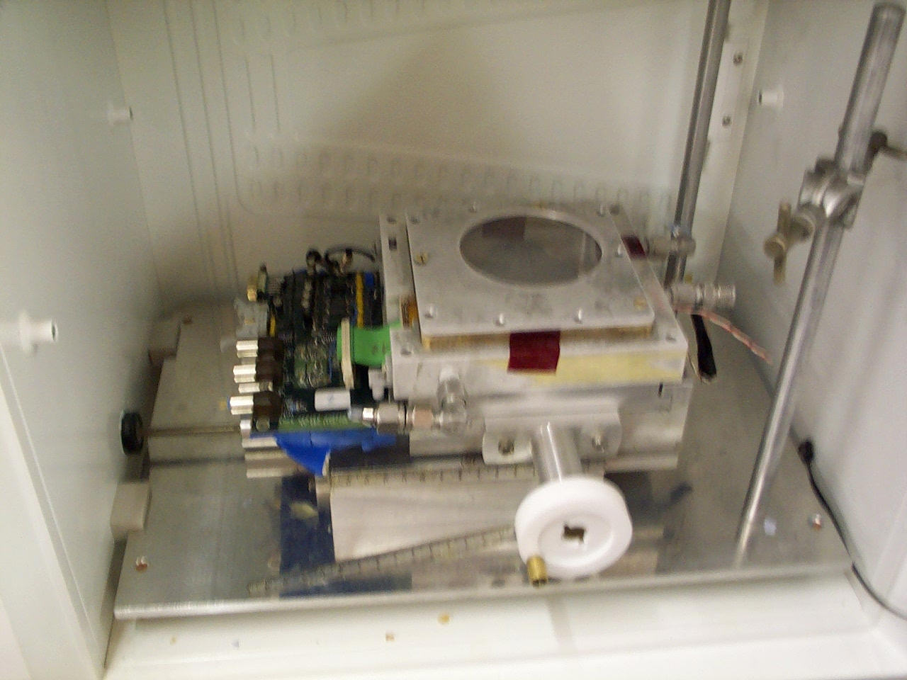
x-y table holding an irradiated LHC-b detector | 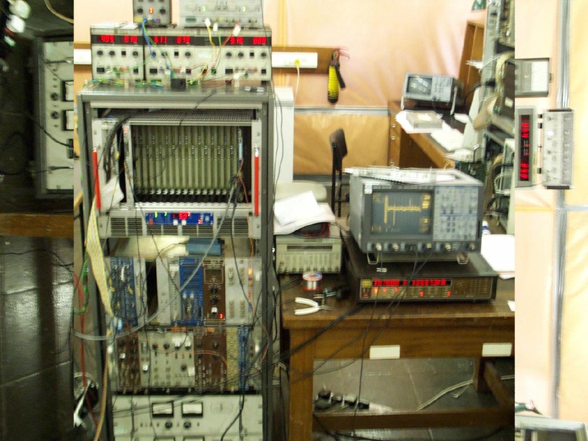
SCT128 data acquisition crate |
|
Before irradiation:
CV of 1728-5 (M. H.) CV of 1728-25 (M. H.) CV of 1729-7 (M. H.) Strip integrity before irradiation (M. H.): 1728-5, 1728-25, 1729-7. |
Results after irradiation (**):
IV's of 1728-25 and 1729-7 Interstrip capacitance; central strip to two nearest neighbours each side Interstrip capacitance; central strip to one nearest neighbour each side, with comparison to pre-irradiation values |
|
|
|
|
RESMDD'04 |
…or the 5th International Conference on Radiation Effects on Semiconductor Materials Detectors and Devices October 10-13, 2004, L.go E. Fermi 2, Florence, Italy You find here the talk. |
|
VCI
2004 |
…or the 10th Vienna Conference on Instrumentation, Vienna, Austria, February 16-21 2004 You find here the poster and the article. |
|
ERICE
2003 |
…or the workshop on Innovative Detectors for Supercolliders, Erice (TP), Italy, 29th Sep.-03 Oct. 2003 You find here the talk and the article. |
|
ELBA
2003 |
…or the 9th Pisa Meeting on Advanced Detectors, La Biodola, Isola d'Elba, 25-31 May 2003 November 3-8, 2002. You find here the poster and the article. |
|
VERTEX
2002 |
…or the 11th INTERNATIONAL WORKSHOP ON VERTEX DETECTORS, Ohana Keauhou Beach Resort, 78-6740 Alii Drive Kailua-Kona, Hawaii November 3-8, 2002. You find here the talk and the article. |
|
ELMAU
2002 |
… or the 9th EUROPEAN SYMPOSIUM ON SEMICONDUCTOR DETECTORS, New Developments on Radiation Detectors, Schloss Elmau, June 23 - 27, 2002. You find here the article. |
|
ISM2E-YS |
... invited talk at the International Symposium of Young Scholars on Mechanical and Material Engineering for Science and Experiments, 11-16th of August 2001 Changsha, Hunan Province, China. Here you can find the transparencies of my talk. |
|
4th STD |
... or the 4th International Symposium on Development and Application of Semiconductor Tracking Detectors (Hiroshima, March 22-25 2000). I have presented a comparative study of oxygenated and control Si diodes, miniature and full-sized microstrip detectors. Here you can find the transparencies of my talk. |
|
RD 99 |
... or the 4th International Conference
on Large Scale Applications and Radiation Hardness of Semiconductor Detectors
(Firenze, Italy, 23-25 June 1999) I have presented some results concerning
changes in interstrip capacitance and noise in microstrip detectors made by
Micron on 6" <100> substrate or by Hamamatsu on 4"
<111> substrate. |
|
Radecs 99 |
....or the 5th EUROPEAN CONFERENCE:
Radiation and its effects on components and systems (Abbaye de Fontevraud,
FRANCE, Maine et Loire, 13 - 17 septembre 1999). |
My ![]() Publication List.
Publication List.
University of Liverpool - Department of Physics Oliver Lodge Laboratory Oxford Street Liverpool L69 7ZE United Kingdom |